
My group’s long-term research mission is to develop advanced nanofabrication and nanomanufacturing technologies that will fabricate nanoscale device structures substantially more advanced than state-of-the-art technology permits as well as create innovative functional devices by combining multidisciplinary knowledge (e.g., Fluid Mechanics, Electronics, Photonics, and Biology) and nanotechnology. Toward this mission, my recent research aims at creating new nanoimprint/nanoprint technologies capable of processing emerging atomically layered two-dimensional (2D) materials (e.g., graphene and transition metal dichalcogenides (TMDCs)) into functional device architectures and leveraging their uniquely advantageous properties for novel device applications in Nanoelectronics, Photonics, and Biosensing.
Current Research Projects
Advanced Nanoimprint Lithography Technology for Manufacturing Applications
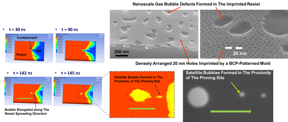
Nanoimprint lithography (NIL) technology has been adopted by the industry as an important candidate technology for patterning functional nanostructures over large areas. However, the current NIL-based manufacturing processes still suffer seriously from various defects, such as trapped gas bubbles, incomplete patterns, and organic contaminants, which have significantly hindered the industrial applications of NIL. In this project, my team and Seagate Technology scientists are building an interdisciplinary university-industry collaborative team to investigate the formation mechanisms of such NIL-related defects. Currently, this interdisciplinary university-industry team is continuing to explore new NIL methods capable of realizing defect-free manufacturing processes.
Nanomanufacturing of Emerging 2D Nanomaterials and Nanodevices
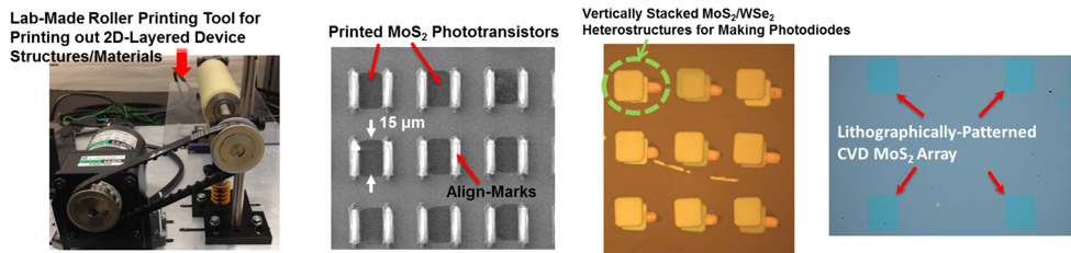
Emerging 2D layer materials, such as graphene, TMDCs (e.g., MoS2, WSe2, and WS2), and topological insulators (e.g., Bi2Se3), recently attracted a great deal of attention because of their attractive electronic, optical, and mechanical properties, versatile chemistry, as well as large natural abundance of relevant bulk materials on the earth. In spite of such desirable properties, the community still lacks the nanomanufacturing capability for producing orderly-arranged, high-quality 2D material-based device structures with a high uniformity in dimension size and electronic/photonic properties over large areas. To tackle this challenge, in the research projects I initiated at the UM, my students and I have worked together to create a series of new upscalable nanoimprint/nanoprint-based technologies dedicated for processing 2D materials into functional device structures.
2D Layer-Based Functional Devices with New Functionalities
In addition to advancing nanomanufacturing capabilities, my team’s recent research also seeks to leverage uniquely advantageous properties of emerging 2D materials for new device applications in nanoelectronics, optoelectronics, energy, and biosensors. Some examples of such device applications are listed below:
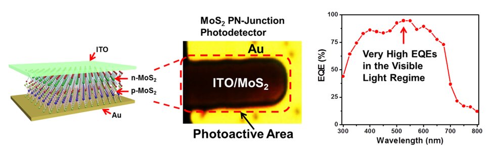
- New photovoltaic (PV) devices based on vertically stacked graphene/MoS2 heterostructures (ACS Nano 8, 5270 (2014) and APL 104, 232103 (2014)). Such PV devices can greatly leverage the superior photonic properties of TMDC layers. Specifically, they exhibit a high photocurrent density up to ~30 mA/cm2, which is comparable to that of high-profile PV cells based on exquisite III-V semiconductors (note that III-V semiconductors are much more expensive than TMDCs). They also exhibit high quantum efficiency >60% over a broad range of wavelengths (NUV-vis-NIR), which breaks the “blue-response-reduction” limit in conventional PVs/photodetectors.
-
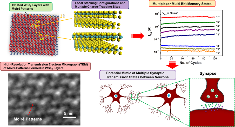
Multi-Bit (or analog-tunable) memory devices: We found that MoS2 transistors, when treated with plasmas, can dramatically serve as low-cost, non-volatile, highly durable memories with multi-bit data storage capability (ACS Nano 8, 4023 (2014)). We have demonstrated binary and 2-bit (or 4-level) data states suitable for year-scale data storage applications. Recently, we further found that mechanically-twisted WSe2 layers (another important 2D semiconductor) with electronic moiré patterns also exhibit multi-bit and even quasi-analog-tunable charge memory states (ACS Nano 11, 1091 (2017)). We anticipate that these two works would provide important scientific insights for leveraging the unique structural property of layered materials in data storage and emerging analog computing applications, and would enable new real-time neuromorphic circuits for neuro-inspired computing systems as well as commercially-viable solid-state drives with a cost/bit at least one order of magnitude lower than that of the current flash memories.
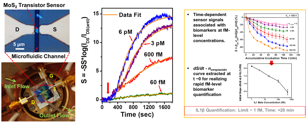
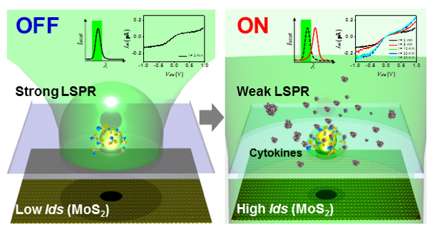
- New nanoelectronics/photonics/nanofluidics-integrated biosensors: We have been performing a series of projects to integrate and operate 2D-material-based nanoelectronic/optoelectronic biosensors in microfluidic environments for detecting/quantifying a series of important low-abundance biomarker molecules associated with precise medicine applications. Especially, in our most recent works, we created new biosensors and biosensing schemes, which can enable rapid (min-scale) quantification of cytokine molecules in complex solutions (serum and saliva) with femtomolar-level detection limits, surpassing most of the conventional cytokine detection schemes in terms of detection limit, sensitivity, and required time. These works advanced the critical device physics for leveraging the excellent electronic properties of 2D semiconductors in biomedical applications and also led to a series of publications (ACS Nano Article ASAP (2017), ACS Sensors 2, 274 (2017), ACS Nano 9, 8773 (2015), JVSTB 33 06FG01 (2015), APL 107, 012105 (2015), Scientific Reports 5, 10546 (2015)). Based on these works, my team is now collaborating with several teams in Engineering and Medical Schools to explore new clinical applications of our biosensors, especially in the fields related to inflammatory diseases, traumatic brain injuries, and translations.
-
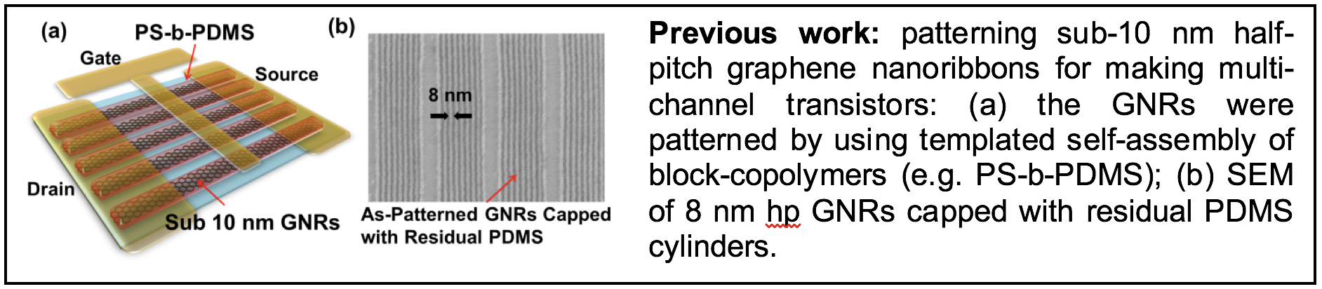
Patterning Densely Arranged Sub-10 nm Graphene Nanoribbons Using Directed Self-Assembly of Block Copolymers for Making Multi-Channel FETs
One of the most exciting and pressing research directions of graphene is to examine how nanolithographic technologies can be adapted, developed, and refined to pattern graphene sheets into nanostructures, in order to obtain the desirable electronic characters and functionalities that leverage the unique property or potential of graphene. Our group is developing new nanofabrication methods to create densely arranged sub-10 nm scale graphene nanoelectronic structures over large areas (ACS Nano, 6, 11, 9700 (2012)).